Realization of high aspect ratio metalenses by facile nanoimprint lithography using water-soluble stamps
doi: 10.1186/s43074-023-00096-2
Realization of high aspect ratio metalenses by facile nanoimprint lithography using water-soluble stamps
-
Abstract:
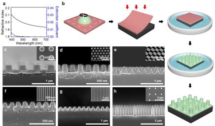
Nanoimprint lithography (NIL) has attracted attention recently as a promising fabrication method for dielectric metalenses owing to its low cost and high throughput, however, high aspect ratio (HAR) nanostructures are required to manipulate the full 2π phase of light. Conventional NIL using a hard-polydimethylsiloxane (h-PDMS) mold inevitably incurs shear stress on the nanostructures which is inversely proportional to the surface area parallel to the direction of detachment. Therefore, HAR structures are subjected to larger shear stresses, causing structural failure. Herein, we propose a novel wet etching NIL method with no detachment process to fabricate flawless HAR metalenses. The water-soluble replica mold is fabricated with polyvinyl alcohol (PVA) which is simpler than an h-PDMS mold, and the flexibility of the PVA mold is suitable for direct printing as its high tensile modulus allows high-resolution patterning of HAR metalenses. The diffraction-limited focusing of the printed metalenses demonstrates that it operates as an ideal lens in the visible regime. This method can potentially be used for manufacturing various nanophotonic devices that require HAR nanostructures at low cost and high throughput, facilitating commercialization.
-
[1] Higgins SG, Becce M, Belessiotis-Richards A, Seong H, Sero JE, Stevens MM. High-aspect-ratio nanostructured surfaces as biological metamaterials. Adv Mater. 2020;32:1903862. https://doi.org/10.1002/adma.201903862. [2] Chiappini C. Nanoneedle-based sensing in biological systems. ACS Sens. 2017;2:1086–102. https://doi.org/10.1021/acssensors.7b00350. [3] Mas-Moruno C, Su B, Dalby MJ. Multifunctional coatings and nanotopographies: toward cell instructive and antibacterial implants. Adv Healthc Mater. 2019;8:1801103. https://doi.org/10.1002/adhm.201801103. [4] Harding FJ, Surdo S, Delalat B, Cozzi C, Elnathan R, Gronthos S, Voelcker NH, Barillaro G. Ordered silicon pillar arrays prepared by electrochemical micromachining: substrates for high-efficiency cell transfection. ACS Appl Mater Interfaces. 2016;8:29197–202. https://doi.org/10.1021/acsami.6b07850. [5] Päivänranta B, Merbold H, Giannini R, Büchi L, Gorelick S, David C, Löffler JF, Feurer T, Ekinci Y. High aspect ratio plasmonic nanostructures for sensing applications. ACS Nano. 2011;5:6374–82. https://doi.org/10.1021/nn201529x. [6] Koenderink AF. Plasmon nanoparticle array waveguides for single photon and single plasmon sources. Nano Lett. 2009;9:4228–33. https://doi.org/10.1021/nl902439n. [7] McFarland AD, Van Duyne RP. Single silver nanoparticles as real-time optical sensors with zeptomole sensitivity. Nano Lett. 2003;3:1057–62. https://doi.org/10.1021/nl034372s. [8] Lyvers DP, Moon JM, Kildishev AV, Shalaev VM, Wei A. Gold Nanorod arrays as plasmonic cavity resonators. ACS Nano. 2008;2:2569–76. https://doi.org/10.1021/nn8006477. [9] McPhillips J, Murphy A, Jonsson MP, Hendren WR, Atkinson R, Höök F, Zayats AV, Pollard RJ. High-performance biosensing using arrays of plasmonic nanotubes. ACS Nano. 2010;4:2210–6. https://doi.org/10.1021/nn9015828. [10] Carstensen MS, Zhu X, Iyore OE, Mortensen NA, Levy U, Kristensen A. Holographic resonant laser printing of metasurfaces using plasmonic template. ACS Photonics. 2018;5:1665–70. https://pubs.acs.org/doi/full/10.1021/acsphotonics.7b01358. [11] Khorasaninejad M, Chen WT, Devlin RC, Oh J, Zhu AY, Capasso F. Metalenses at visible wavelengths: diffraction-limited focusing and subwavelength resolution imaging. Science. 2016;352:1190–4. https://www.science.org/doi/10.1126/science.aaf6644. [12] Ren H, Fang X, Jang J, Bürger J, Rho J, Maier SA. Complex-amplitude metasurface-based orbital angular momentum holography in momentum space. Nat Nanotechnol. 2020;15:948–55. https://doi.org/10.1038/s41565-020-0768-4. [13] Chen WT, Zhu AY, Sanjeev V, Khorasaninejad M, Shi Z, Lee E, Capasso FA. Broadband achromatic metalens for focusing and imaging in the visible. Nat Nanotechnol. 2018;13:220–6. https://doi.org/10.1038/s41565-017-0034-6. [14] Jung C, Kim G, Jeong M, Jang J, Dong Z, Badloe T, Yang JKW, Rho J. Metasurface-driven optically variable devices. Chem Rev. 2021;121:13013–50. https://doi.org/10.1021/acs.chemrev.1c00294. [15] Hu J, Bandyopadhyay S, Liu YH, Shao LY. A Review on Metasurface: From Principle to Smart Metadevices. Front Phys. 2021;8:586087. https://doi.org/10.3389/fphy.2020.586087. [16] Arbabi A, Arbabi E, Horie Y, Kamali SM, Faraon A. Planar metasurface retroreflector. Nat Photonics. 2017;11:415–20. https://doi.org/10.1038/nphoton.2017.96. [17] Zheng G, Mühlenbernd H, Kenney M, Li G, Zentgraf T, Zhang S. Metasurface holograms reaching 80% efficiency. Nat Nanotechnol. 2015;10:308–12. https://doi.org/10.1038/nnano.2015.2. [18] Yu N, Capasso F. Flat optics with designer metasurfaces. Nat Mater. 2014;13:139–50. https://doi.org/10.1038/nmat3839. [19] Kim J, Jeon D, Seong J, Badloe T, Jeon N, Kim G, Kim J, Baek S, Lee JL, Rho J. Photonic encryption platform via dual-band vectorial metaholograms in the ultraviolet and visible. ACS Nano. 2022;16:3546–53. https://doi.org/10.1021/acsnano.1c10100. [20] Badloe T, Kim J, Kim I, Kim WS, Kim WS, Kim YK, Rho J. Liquid crystal-powered mie resonators for electrically tunable photorealistic color gradients and dark blacks. Light Sci Appl. 2022;11:1–11. https://doi.org/10.1038/s41377-022-00806-8. [21] Kim J, Kim W, Oh DK, Kang H, Kim H, Badloe T, Kim S, Park C, Choi H, Lee H, Rho J. One-step printable platform for high-efficiency metasurfaces down to the deep-ultraviolet region. Light Sci Appl. 2023;12:68. https://doi.org/10.1038/s41377-023-01086-6. [22] Kim J, Yang Y, Badloe T, Kim I, Yoon G, Rho J. Geometric and physical configurations of meta-atoms for advanced metasurface holography. InfoMat. 2021;3:739–54. https://doi.org/10.1002/inf2.12191. [23] Kim I, Yoon G, Jang J, Genevet P, Nam KT, Rho J. Outfitting next generation displays with optical metasurfaces. ACS Photonics. 2018;5:3876–95. https://doi.org/10.1021/acsphotonics.8b00809. [24] Lin D, Fan P, Hasman E, Brongersma ML. Dielectric gradient metasurface optical elements. Science. 2014;345:298–302. https://www.science.org/doi/10.1126/science.1253213. [25] So S, Kim J, Badloe T, Lee C, Yang Y, Kang H, Rho J. Multicolor and 3D holography generated by inverse-designed single-cell metasurfaces. Adv Mater. 2022;27;2208520. https://doi.org/10.1002/adma.202208520. [26] Ko B, Badloe T, Yang Y, Park J, Kim J, Jeong H, Jung C, Rho J. Tunable metasurfaces via the humidity responsive swelling of single-step imprinted polyvinyl alcohol nanostructures. Nat Commun. 2022;13;6256. https://doi.org/10.1038/s41467-022-34566-1. [27] Zhu X, Czolkos I, Johansson A, Nielsen T, Kristensen A. Master origination by 248 nm DUV lithography for plasmonic color generation. Appl Phys Lett. 2021;118:141103. https://doi.org/10.1063/5.0046163. [28] Yu YF, Zhu AY, Paniagua-Domínguez R, Fu YH, Luk’yanchuk B, Kuznetsov AI. High-Transmission Dielectric Metasurface with 2π Phase Control at Visible Wavelengths. Laser Photonics Rev. 2015;9:412–8. https://doi.org/10.1002/lpor.201500041. [29] Devlin RC, Khorasaninejad M, Chen WT, Oh J, Capasso F. Broadband high-efficiency dielectric metasurfaces for the visible spectrum. Proc Natl Acad Sci. 2016;113:10473–8. https://doi.org/10.1073/pnas.1611740113. [30] Kim J, Oh DK, Kim H, Yoon G, Jung C, Kim J, Badloe T, Kang H, Kim S, Yang Y, Lee J, Ko B, Ok JG, Rho J. Metasurface holography reaching the highest efficiency limit in the visible via one-step nanoparticle-embedded-resin printing. Laser Photonics Rev. 2022;16:2200098. https://doi.org/10.1002/lpor.202200098. [31] Yoon G, Kim I, Rho J. Challenges in fabrication towards realization of practical metamaterials. Microelectron Eng. 2016;163:7–20. https://doi.org/10.1016/j.mee.2016.05.005. [32] Wu W, Yu Z, Wang SY, Williams RS, Liu Y, Sun C, Zhang X, Kim E, Shen YR, Fang NX. Midinfrared metamaterials fabricated by nanoimprint lithography. Appl Phys Lett. 2007;90:063107. https://doi.org/10.1063/1.2450651. [33] Chanda D, Shigeta K, Gupta S, Cain T, Carlson A, Mihi A, Baca AJ, Bogart GR, Braun P, Rogers JA. Large-area flexible 3D optical negative index metamaterial formed by nanotransfer printing. Nat Nanotechnol. 2011;6:402–7. https://doi.org/10.1038/nnano.2011.82. [34] Byeon KJ, Lee H. Recent progress in direct patterning technologies based on nano-imprint lithography. Eur Phys J Appl Phys. 2012;59.https://doi.org/10.1051/EPJAP/2012120166. [35] Hong SH, Bae BJ, Yang KY, Jeong JH, Kim HS, Lee H. Fabrication of sub-50 nm Au nanowires using thermally curing nanoimprint lithography. Electron Mater Lett. 2009;5:139–43. https://doi.org/10.3365/eml.2009.12.139. [36] Guo LJ. Nanoimprint lithography: methods and material requirements. Adv Mater. 2007;19:495–513. https://doi.org/10.1002/adma.200600882. [37] Yoon G, Kim K, Huh D, Lee H, Rho J. Single-step manufacturing of hierarchical dielectric metalens in the visible. Nat Commun. 2020;11:1–10. https://doi.org/10.1038/s41467-020-16136-5. [38] Yoon G, Kim K, Kim SU, Han S, Lee H, Rho J. Printable nanocomposite metalens for high-contrast near-infrared imaging. ACS Nano. 2021;15:698–706. https://doi.org/10.1021/acsnano.0c06968. [39] Kim K, Yoon G, Baek S, Rho J, Lee H. Facile nanocasting of dielectric metasurfaces with Sub-100 nm resolution. ACS Appl Mater Interfaces. 2019;11:26109–15. https://doi.org/10.1021/acsami.9b07774. [40] Greiner C, Del Campo A, Arzt E. Adhesion of bioinspired micropatterned surfaces: effects of pillar radius, aspect ratio, and preload. Langmuir. 2009;23:3495–502. https://doi.org/10.1021/la0633987. [41] Brörmann K, Burger K, Jagota A, Bennewitz R. Discharge during detachment of micro-structured PDMS sheds light on the role of electrostatics in adhesion. J Adhes. 2012;88:589–607. https://doi.org/10.1080/00218464.2012.682897. [42] Mukherjee R, Patil GK, Sharma A. Solvent vapor-assisted imprinting of polymer films coated on curved surfaces with flexible PVA stamps. Ind Eng Chem Res. 2009;48:8812–8. https://doi.org/10.1021/ie801740y. [43] Schaper CD, Miahnahri A. Polyvinyl alcohol templates for low cost, high resolution, complex printing. J Vac Sci Technol B. 2004;22:3323–6. https://doi.org/10.1116/1.1827218. [44] Hwang SY, Hong SH, Jung HY, Lee H. Fabrication of roll imprint stamp for continuous UV roll imprinting process. Microelectron Eng. 2009;86:642–5. https://doi.org/10.1016/j.mee.2008.11.05542. [45] Qin D, Xia Y, Whitesides GM. Soft lithography for micro- and nanoscale patterning. Nat Protoc. 2010;5:491. https://doi.org/10.1038/nprot.2009.234. [46] Delamarche E, Schmid H, Michel B, Biebuyck H. Stability of molded polydimethylsiloxane microstructures. Adv Mater. 1997;9:741–6. https://doi.org/10.1002/adma.19970090914. [47] Jung GY, Li Z, Wu W, Chen Y, Olynick DL, Wang SY, Tong WM, Williams RS. Vapor-phase self-assembled monolayer for improved mold release in nanoimprint lithography. Langmuir. 2005;21:1158–61. https://doi.org/10.1021/la0476938. [48] Shen F, Wang A. Fast-fourier-transform based numerical integration method for the rayleigh-sommerfeld diffraction formula. Appl Opt. 2006;45:1102–10. https://doi.org/10.1364/AO.45.001102. [49] Kim J, Seong J, Kim W, Lee GY, Kim S, Kim H, Moon SW, Oh DK, Yang Y, Park J, Jang J, Kim Y, Jeong M, Park C, Choi H, Jeon G, Lee Ki, Yoon DH, Park N, Lee B, Lee H, Rho J. Scalable manufacturing of high-index atomic layer-polymer hybrid metasurfaces for metaphotonics in the visible. Nat Mater. 2023;22:474–81. [50] Choi KM, Rogers JA. A photocurable poly (dimethylsiloxane) chemistry designed for soft lithographic molding and printing in the nanometer regime. J Am Chem Soc. 2003;125:4060–1. https://doi.org/10.1021/ja029973k. [51] Ulman A. Formation and structure of self-assembled monolayers. Chem Rev. 1996;96:1533–54. https://doi.org/10.1021/cr9502357. [52] Schreiber F. Structure and growth of self-assembling monolayers. Prog Surf Sci. 2000;65:151–257.https://doi.org/10.1016/S0079-6816(00)00024-1.
 下载:
下载:
 点击查看大图
计量
- 文章访问数: 211
- HTML全文浏览量: 3
- PDF下载量: 10
- 被引次数: 0